- English
- Español
- Português
- русский
- Français
- 日本語
- Deutsch
- tiếng Việt
- Italiano
- Nederlands
- ภาษาไทย
- Polski
- 한국어
- Svenska
- magyar
- Malay
- বাংলা ভাষার
- Dansk
- Suomi
- हिन्दी
- Pilipino
- Türkçe
- Gaeilge
- العربية
- Indonesia
- Norsk
- تمل
- český
- ελληνικά
- український
- Javanese
- فارسی
- தமிழ்
- తెలుగు
- नेपाली
- Burmese
- български
- ລາວ
- Latine
- Қазақша
- Euskal
- Azərbaycan
- Slovenský jazyk
- Македонски
- Lietuvos
- Eesti Keel
- Română
- Slovenski
- मराठी
- Srpski језик
Differences Between Vacuum Chucks and Electrostatic Chucks
As the indispensable core links in semiconductor manufacturing, the stability and precision of wafer holding technology directly impact on chip production efficiency and finished device quality. Vacuum chucks and electrostatic chucks are the two mainstream wafer holding solutions for semiconductor manufacturing. Though both belong to wafer chucks, they differ greatly in structure, performance characteristics and applicable scenarios.
1. Different Working Principles
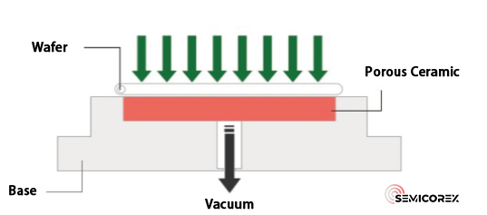
Vacuum chucks rely on negative pressure to hold wafers in place. Air is extracted via pipelines connected to a vacuum pump, forming negative pressure underneath the wafer to firmly attach wafers or substrates to the chuck surface. Chuck’s base is precision-machined from ceramic or metal, and its adsorption surface consists of a porous ceramic plate fitted into a counterbore on the base, with its periphery bonded and sealed to the base. Connected to a vacuum pump through internal microporous channels of the ceramic plate, the chuck generates a vacuum zone far below atmospheric pressure, thus securing the wafer tightly.
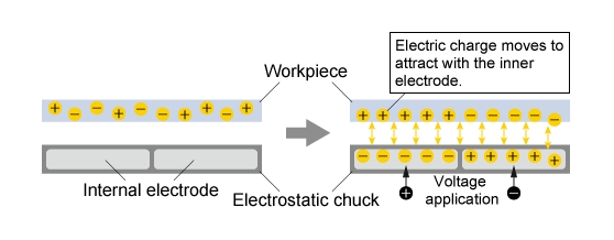
Electrostatic chucks adopt a core structure with electrodes embedded inside a metal base, covered by a high-performance ceramic dielectric layer. They generate an electrostatic field on their surface to induce electric charges on workpieces, creating electrostatic attraction to clamp wafers or substrates. When voltage is applied, a strong electrostatic field forms between the electrodes, ceramic dielectric and wafer, delivering holding force of several thousand to tens of thousands Pascals for stable wafer fixation.
2. Different Performance Advantages
Vacuum chucks are compatible with wafers of different dimensions and various process workflows, delivering stable fixation of wafers during processing. Compared with electrostatic chucks, they feature low manufacturing and maintenance costs owing to their relatively simple internal structures.
However, when wafers undergo processes requiring operation in a vacuum or low-pressure environment, such as chemical vapor deposition, vacuum chucks relying on pressure differences cannot meet process requirements. Furthermore, when wafers are held in place by vacuum chucks, air pressure may cause the wafer to deform, resulting in a rebound after processing. This may result in a wavy surface, poor flatness and reduced machining accuracy on the processed wafer.
Electrostatic chucks adopt contactless adsorption, offering consistent, evenly distributed clamping force. This effectively prevents wafer warping, distortion and damage, preserving excellent flatness for higher machining accuracy. Equipped with helium backside cooling for uniform temperature distribution, electrostatic chucks support accurate wafer temperature regulation.
On the downside, electrostatic chucks have complex structures with extremely strict standards for surface flatness, smoothness and micron-scale microstructures. Micron-level precision for micro-features creates high technical barriers in raw material formulation, sintering and surface finishing. Temperature control remains a core technical challenge; aluminum nitride (AlN) dielectric ESCs for enhanced heat dissipation involve even more complicated production processes. Stringent multi-dimensional technical requirements drive up the product price, and regular inspection and maintenance of electrostatic systems are mandatory to guarantee stable operation.
3. Different Main Application Fields
With high flatness, superior parallelism, dense uniform texture, high mechanical strength, uniform air permeability and easy reconditioning, vacuum chucks are used to fix and transport flat, well-sealed workpieces such as metal sheets and plastic substrates. Within semiconductor manufacturing, they serve wafer thinning, dicing, grinding, cleaning and other wafer treatment processes, effectively resolving common issues including wafer indentations, electrostatic breakdown of chips and particle contamination.
Designed for flat, non-conductive workpieces, electrostatic chucks are ultra-clean wafer carriers dedicated to vacuum and plasma environments. They are widely deployed in plasma and vacuum semiconductor processes, including dry etching, PECVD, thermal CVD, physical vapor deposition (PVD), ion implantation and extreme ultraviolet lithography (EUVL).