
- English
- Español
- Português
- русский
- Français
- 日本語
- Deutsch
- tiếng Việt
- Italiano
- Nederlands
- ภาษาไทย
- Polski
- 한국어
- Svenska
- magyar
- Malay
- বাংলা ভাষার
- Dansk
- Suomi
- हिन्दी
- Pilipino
- Türkçe
- Gaeilge
- العربية
- Indonesia
- Norsk
- تمل
- český
- ελληνικά
- український
- Javanese
- فارسی
- தமிழ்
- తెలుగు
- नेपाली
- Burmese
- български
- ລາວ
- Latine
- Қазақша
- Euskal
- Azərbaycan
- Slovenský jazyk
- Македонски
- Lietuvos
- Eesti Keel
- Română
- Slovenski
- मराठी
- Srpski језик

Epitaxial Layers: The Foundation of Advanced Semiconductor Devices
Figure 1: Illustrates the correlation between doping concentrations, layer thickness, and breakdown voltage for unipolar devices.

The preparation of SiC epitaxial layers primarily encompasses techniques such as Evaporation Growth, Liquid Phase Epitaxy (LPE), Molecular Beam Epitaxy (MBE), and Chemical Vapor Deposition (CVD), with CVD being the predominant method for mass production in factories.
Table 1: Provides a comparative overview of the main epitaxial layer preparation methods.

A groundbreaking approach involves growth on off-axis {0001} substrates at a specific tilt angle, as depicted in Figure 2(b). This method significantly increases step density while reducing step size, facilitating nucleation primarily at step bunching sites and thus, allowing the epitaxial layer to perfectly replicate the substrate’s stacking sequence, eliminating the coexistence of polytypes.
Figure 2: Demonstrates the physical process of step-controlled epitaxy in 4H-SiC.
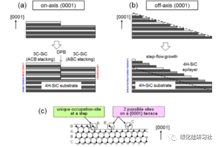
Figure 3: Shows the critical conditions for CVD growth in step-controlled epitaxy for 4H-SiC.
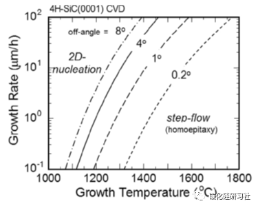
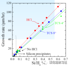
Figure 4: Compares growth rates under different silicon sources for 4H-SiC epitaxy.
In the realm of low and medium voltage applications (e.g., 1200V devices), SiC epitaxy technology has reached a mature stage, offering relatively superior uniformity in thickness, doping concentration, and defect distribution, adequately meeting the requirements for low and medium-voltage SBD, MOS, JBS devices, and others.
However, the high-voltage domain still presents significant challenges. For instance, devices rated at 10000V require epitaxial layers approximately 100μm thick, but these layers exhibit considerably poorer thickness and doping uniformity compared to their low-voltage counterparts, not to mention the detrimental impact of triangular defects on overall device performance. High-voltage applications, which tend to favor bipolar devices, also place stringent demands on minority carrier lifetime, necessitating process optimization to enhance this parameter.
Currently, the market is dominated by 4-inch and 6-inch SiC epitaxial wafers, with a gradual increase in the proportion of large-diameter SiC epitaxial wafers. The size of SiC epitaxial wafers is fundamentally determined by the dimensions of SiC substrates. With 6-inch SiC substrates now commercially available, the transition from 4-inch to 6-inch SiC epitaxy is steadily underway.
As SiC substrate fabrication technology advances and production capacities expand, the cost of SiC substrates is progressively decreasing. Given that substrates account for more than 50% of the cost of epitaxial wafers, the decreasing substrate prices are expected to lead to lower costs for SiC epitaxy, thereby promising a brighter future for the industry.**


