
- English
- Español
- Português
- русский
- Français
- 日本語
- Deutsch
- tiếng Việt
- Italiano
- Nederlands
- ภาษาไทย
- Polski
- 한국어
- Svenska
- magyar
- Malay
- বাংলা ভাষার
- Dansk
- Suomi
- हिन्दी
- Pilipino
- Türkçe
- Gaeilge
- العربية
- Indonesia
- Norsk
- تمل
- český
- ελληνικά
- український
- Javanese
- فارسی
- தமிழ்
- తెలుగు
- नेपाली
- Burmese
- български
- ລາວ
- Latine
- Қазақша
- Euskal
- Azərbaycan
- Slovenský jazyk
- Македонски
- Lietuvos
- Eesti Keel
- Română
- Slovenski
- मराठी
- Srpski језик

Application Scenarios for Epitaxial Layers
We know that further epitaxial layers need to be built on top of some wafer substrates for device fabrication, typically LED light-emitting devices, which require GaAs epitaxial layers on top of silicon substrates; SiC epitaxial layers are grown on top of conductive SiC substrates for building devices such as SBDs, MOSFETs, etc. for high voltage, high current and other power applications; GaN epitaxial layers are built on top of semi-insulating SiC substrates for building HEMTs and other RF applications. The GaN epitaxial layer is built on top of the semi-insulated SiC substrate to further construct HEMT devices for RF applications such as communication.
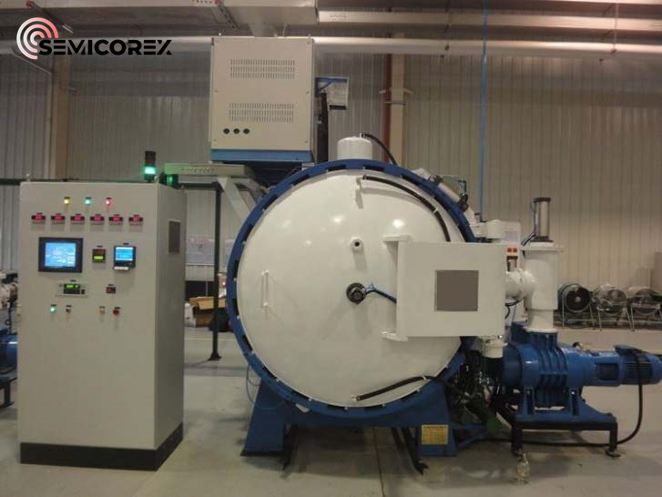
Here it is necessary to use CVD equipment (of course, there are other technical methods). Metal Organic Chemical Vapor Deposition (MOCVD) is to use Group III and II elements and Group V and VI elements as the source materials and deposits them on the substrate surface by thermal decomposition reaction to grow various thin layers of Group III-V (GaN, GaAs, etc.), Group II-VI (Si, SiC, etc.) and multiple solid solutions. and multi-layer solid solutions of thin single-crystal materials are the main means of producing optoelectronic devices, microwave devices, power device materials.
Previous:Discussing CVD furnace


