
- English
- Español
- Português
- русский
- Français
- 日本語
- Deutsch
- tiếng Việt
- Italiano
- Nederlands
- ภาษาไทย
- Polski
- 한국어
- Svenska
- magyar
- Malay
- বাংলা ভাষার
- Dansk
- Suomi
- हिन्दी
- Pilipino
- Türkçe
- Gaeilge
- العربية
- Indonesia
- Norsk
- تمل
- český
- ελληνικά
- український
- Javanese
- فارسی
- தமிழ்
- తెలుగు
- नेपाली
- Burmese
- български
- ລາວ
- Latine
- Қазақша
- Euskal
- Azərbaycan
- Slovenský jazyk
- Македонски
- Lietuvos
- Eesti Keel
- Română
- Slovenski
- मराठी
- Srpski језик

Dry Etching vs Wet Etching
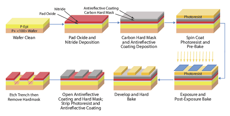
In semiconductor fabrication, etching is one of the major steps, along with photolithography and thin-film deposition. It involves removing unwanted materials from the surface of a wafer using chemical or physical methods. This step is carried out after coating, photolithography, and developing. It is used to remove the exposed thin film material, leaving only the desired portion of the wafer, and then removing the excess photoresist. These steps are repeated numerous times to create complex integrated circuits.
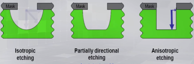
Etching is classified into two categories: dry etching and wet etching. Dry etching involves using reactive gases and plasma etching, while wet etching involves immersing the material in a corrosion solution to corrode it. Dry etching allows for anisotropic etching, which means that only the vertical direction of the material is etched without affecting the transverse material. This ensures the transfer of small graphics with fidelity. In contrast, wet etching is not controllable, which can reduce the width of the line or even destroy the line itself. This results in poor quality production chips.
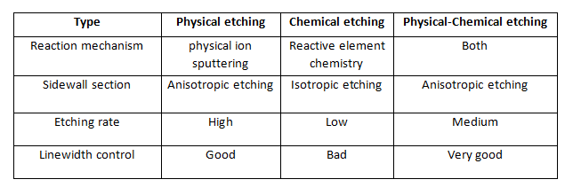
Dry etching is classified into physical etching, chemical etching, and physical-chemical etching based on the ion etching mechanism used. Physical etching is highly directional and can be anisotropic etching, but not selective etching. Chemical etching uses plasma in the chemical activity of the atomic group and the material to be etched to achieve the purpose of etching. It has good selectivity, but anisotropy is poor due to the core of the etching or chemical reaction.
Previous:Dislocation in SiC crystals


